A NAND gate (NOT- AND) is one kind of logic gate that works like an AND gate through a NOT gate. Here, the output of the AND gate can be inverted through the NOT gate. As a result, when all the inputs of a NAND gate are HIGH then only it gives a LOW output. These gates are used to design an extensive range of logic functions like D Flip-Flops & SR Latches. So this article discusses an overview of a CD4011 NAND Gate and its working.
What is CD4011 NAND Gate?
CD4011 IC is a quadrable two-input NAND gate IC that includes four NAND gates within a single chip. The logic used by this gate isCMOSwhere designing of all the inputs and outputs can be done based on the voltage level of CMOS logic.
This IC is used to perform NAND logic otherwise you can utilize a combination of 4 logic gates to achieve AND/OR operation also. CD4011 NAND gate ICs offer the system designer through direct execution of the NAND gate function & supplement the existing CMOS, gate family.
These ICs are available in different packages like 14-lead hermetic DIL (dual-in-line) ceramic, 14-lead DIL plastic, 14-lead small-outline & 14-lead thin shrink tiny outline packages.
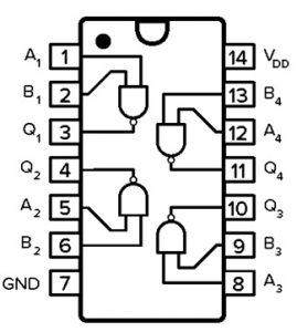
Pin Configuration
The pin configuration of the CD4011 NAND Gate is shown below. This IC includes 14 pins where each pin and its function are discussed below.
CD4011 IC Pin Configuration
Pin1 (INPUT A): This pin is the input A of the 1st NAND gate
Pin2 (INPUT B): This pin is the input B of the 1st NAND gate
Pin3 (OUTPUT J): This is an o/p J pin of the 1st NAND gate
Pin4 (OUTPUT K): This is an o/p K pin of the second NAND gate
Pin5 (INPUT C): This is the Input C pin of the second NAND gate
Pin6 (INPUT D): This is the Input D pin of the second NAND gate
Pin7 (GND): This is GND pin
Pin8 (INPUT E): This is an Input E pin of the third NAND gate
Pin9 (INPUT F): This is an Input F pin of the third NAND gate
Pin10 (OUTPUT L): This pin is an Output L pin of the third NAND gate
Pin11 (OUTPUT M): This is an Output pin M of the fourth NAND gate
Pin12 (INPUT G): This is an Input pin G of the fourth NAND gate
Pin13 (INPUT H): This is an Input H pin of the fourth NAND gate
Pin14 (VCC/VDD): This pin connects with a 5V power supply
Specifications & Features:
Thefeatures and specifications of CD4011 NAND Gateinclude the following.
2- Input NAND Gate with Quad Package
The operating voltage is 5V
The high range o/p current is 1.5 mA
The low range o/p current is 1.5mA
Time taken for propagation delay is 60 ns
The range of operating temperature is – 55 C to + 125 C
Available packages are 14-pin GDIP, PDIP & PDSO
The propagation delay time is 60 ns
Buffered i/ps & o/ps
Consistent symmetrical o/p characteristics
Input current Max 1µA at 18 V on complete package temperature range and 100 nA at 25°C & 18 V
At 20V of quiescent current, it is 100% tested
Parametric ratings are 5V, 10V & 15V
Mounting type is through-hole
400B series
CMOS technology
Dual terminal position
NAND logic function
CD4011B Part number
CD4000 Technology Family
Min VCC is 3V
Max VCC is 18V
4 Channels
Inputs for each channel -2
Max current to the pin is 6.8 mA
Max current from the pin is –6.8 mA
The type of input is typical CMOS
The type of output is Push-Pull
Standard Speed is > 50ns
Max data rate is 8 Mbps
Range of operating temperature range is -55 to 125 C
Alternatives & Equivalents CD4011 NAND Gates are NTE4011, HCF4011, MC14011, HEF4011 or TC4011. Alternative ICs with two input NAND gates are ; 4572, 4093, 40107, 74HC00, 74HC01 & 74HC03.
How to use CD4011 NAND Gate?
As we have already discussed NAND gate. So, CD4011 IC includes 4 NAND gates. The tabular form and its logic functions are given below.
Input
Input
Output
L
L
H
L
H
H
H
L
H
H
H
L
According to the above tabular form, we can conclude that if both the inputs are high then only the output is low otherwise it is high.
CD4011 IC includes 12 I/O pins for a total of 4 NAND gates. So this IC can be used simply by simply connecting the VDD pin to the positive pin whereas the negative supply is to the GND pin.
This IC operates with +5V where the output voltage of this chip on the o/p will be equivalent to the operating voltage of this chip. Some of the versions of NAND gate ICs will work upto 20V. In the above CD4011 NAND gate IC, the input pins are denoted with A & B whereas the output pins are denoted with ‘Q’.
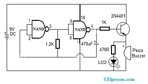
The application circuit diagram of the CD4011 NAND Gate namely the beeper circuit is shown below. In the above beeper circuit, two CD4011 NAND gates play a crucial role. This circuit is very simple to design and used to generate beep sound where indication and alarm are required in such places as hospitals, Fire brigade stations, police stations, etc.
These circuits are very simple to design, use and need less maintenance. So this beeper circuit is designed with a CD4011 two Input NAND gate IC.
Beeper Circuit using CD4011 NAND Gate IC
The required components to build this beeper circuit mainly includes a breadboard, 9V battery, connecting wires, CD4011 IC, 2N4401 NPN Transistor, PiezoBuzzer, 470uF capacitor, 5mm LED & Resistors like 1k,1.2k & 470 ohm.
This NAND gate IC is used in differentelectronic circuitsas it performs like a NAND gate. Once you want to utilize it like a logic inverter, then NAND gates within this IC are connected to work like a NOT gate. So, it is utilized wherever NAND operation with high-speed is required. This IC includes a less transition time that is required for high-speed-based applications.
In the above circuit, the two NAND gate ICs are connected like an astablemultivibratorbecause the o/p at pin-4 of this IC constantly goes low & high. This is continuously turned ON & OFF the transistor to drive the piezoelectric buzzer. Thus, this buzzer will generate a beep sound & the light-emitting diode in the circuit will blink continuously.
This beeper circuit is used in timers, alarm devices for alarming and indicating purposes.
Where to use CD4011 NAND Gate?
As per the previous discussion, CD4011 NAND gate IC includes four NAND logic gates. These gates help in implementing other logic gates like AND, OR & NOT. This IC is applicable where high-speed NAND gate output is necessary because this IC provides output in below 60ns.
For making a high-speed process, we need a circuit always through less transition time. So, it is suggested logic gate is used in high-frequency systems. Theapplications of CD4011 NAND Gateinclude the following.
Decoders
Safety thermostats
Multiplexers
Digital locks
Logic gates
Transmitters & receivers based on AV
Audio players
Portable Audio Docks
AV Receivers
MP3 Players/Recorders
Home Theaters
Used within Blu-Ray Players
PDAs or Personal Digital Assistants (PDAs)
Thus, this is all about an overview of theCD4011 NAND Gate datasheet. This IC belongs to the series of CD40xx CMOS and this IC is available with 4 separate NAND gates. This NAND gate IC is extensively used in several electrical circuits and this IC can be used as a logic inverter by connecting this gate to NOT gate. For high-speed applications, this IC is apt due to the low transition time.
CD4011 Quad 2-Input NAND Gate
Default Title
Robot Pi Shop
Pickup available,usually ready in 1 hour
Ground Floor Shop, Sayde Street, Fanar Matn 1202 Fanar Lebanon